sábado, 24 de julio de 2010

Defects in Dilute Nitrides

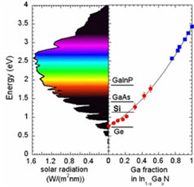
Dilute nitrides, derived from conventional III-V semiconductors such as Ga(In,Al)P and Ga(In)As by insertion of N into the group-V sublattice, have gained increasingly high interest during the last few years. They exhibit unusual and fascinating new physical properties, such as a giant band-gap bowing that allows widely extended band structure engineering. The high interest has also been driven by potential technological advantages provided by the novel dilute nitrides in lattice matching to GaAs and Si substrates. A combination of the remarkable fundamental properties with the technological advantages has provided an unprecedented opportunity to tailor material properties for desired device applications in optoelectronics and photonics, such as improved solid-state lasers for fiber-optic communications, multi-junctional solar cells, integration of efficient III- V optoelectronics with microelectronics based on silicon.

Unfortunately, epitaxial growth of dilute nitrides remains as a great chal-lenge. The required non-equilibrium growth conditions together with the disparity between N and the replaced group-V atoms are known to favor formation of various defects. As the optical quality of dilute nitrides has been shown to deteriorate with increasing N composition, even in the best available materials that are free of structural defects, there is currently a great need in identifying growin point defects and in assessing their role in non-radiative carrier recombination. In fact, Below we shall provide a brief review of our recent results from optically detected magnetic resonance (ODMR) studies of grownin non-radiative defects in Ga(In)NAs and Ga(Al,In)NP, in an effort to provide chemical identi¯cation and experimental signatures of defects and to evaluate their role in carrier recombination. Among them, defect complexes involving intrinsic defects such as antisites and self-interstitials have been positively identifyed and effects of growth conditions, chemical compositions and post-growth processing on formation of the defects have been studied. Non-radiative defects can be monitored using the ODMR technique because a magnetic resonance induced increase in efficiency of dominant non-radiative recombination channels can lead to a corresponding decrease in free carrier concentration available for radiative recombination and thus to a decrease in photoluminescence (PL) intensity.

the issue of defects is one of main problems we are currently facing that hinders a rapid progress of dilute nitrides for various device applications in optoelectronics and photonics. For example, it has been shown that about 50% of threshold current in the best available 1.3 um GaInNAs lasers has been found to be due to defect-related non-radiative recombination channels. Many key parameters of GaInNAs for solar-cell applications have also been found to be limited by defects. Identifying and understanding of the relevant defects in dilute nitrides and designing strategies to eliminate them are therefore crucial to the success of these materials for optoelectronic device applications.

Experimental evidence for the existence of AsGa antisites in Ga(In)NAs alloys grown by gas source molecular beam epitaxy (GS-MBE) has been provided by the ODMR measurements. The participation of an As atom in the defect was concluded from the experimentally resolved hyperfine (hf) structure, i.e. a group of four ODMR lines, characteristic of the hf interaction between an unpaired electron spin S = 1/2 and the nuclear spin I = 3/2 of the 75 As atom (100% natural abundance) | Fig. 1. The hf splitting parameter, A = 737 x 10^4 cm^1, and the g-value of the unpaired electron localized at the defect, g = 2, were determined by fitting experimental data with the effective spin Hamiltonian


The first and second terms in Eq. (1) are the electron Zeeman and hyperfine interaction terms, respectively; ¹B denotes the Bohr magneton. The obtained A value is about 20% smaller than that known for the isolated AsGa in GaAs, suggesting that the revealed defect is a complex involving AsGa. The microscopic structure of the complex does not depend on the N composition in the GaNxAs1¡x layers for x = 1-3%, as the defect parameters do not change with x.

Fuente:
http://przyrbwn.icm.edu.pl/APP/PDF/108/a108z404.pdf

Gerald Soto, CRF 2010-1.
http://gerald-ees.blogspot.com/


Reducing GaN HEMT degradation with InAlN barrier

By using indium aluminum nitride (InAlN) rather than the more usual aluminum gallium nitride (AlGaN) as the barrier layer, one can lattice match (In0.17Al0.83N) with the underlying gallium nitride (GaN), removing strain effects. It is found that spontaneous polarization in the nitride semiconductor materials is sufficient to create the two-dimensional electron gas (2DEG) channel at the barrier/substrate interface that is necessary for HEMT operation. In other words, one does not need strain-induced (piezoelectric) polarization from a mismatched barrier to produce GaN HEMTs.

While strain can produce desirable effects in some semiconductors, such as increased mobility in certain directions, it can also lead to unstable structures that can fail under electrical and thermal stress. Among the achievements for InAlN/GaN HEMTs have been drain current densities exceeding 3A/mm and HEMT operation at 1000°C without permanent damage.
Figure 1: Comparisons of normalized drain current (a), intrinsic channel resistance (b), and threshold voltage (c) after negative gate bias (NGB), off, and semi-on stresses at the same drain-gate potential VDG. VGS=–3V during semi-on stresses. Corresponding bias conditions are VDG =–VG=VDS – VGS.


The researchers from the Technische Universität Wien (TU Vienna), Institute of Electrical Engineering Slovak Academy of Sciences and École Polytechnique Fédérale de Lausanne (EPFL) aimed to fill the gap in the analysis of possible degradation mechanisms in InAlN/GaN HEMTs at various device working points and electrical stressing conditions in a similar way to other groups studying AlGaN/GaN devices. The team also hoped to confirm its expectation that the absence of strain in InAlN can reduce some device degradation processes.

The epitaxial layers (10nm InAlN/1nm AlN/1μm GaN/150nm AlN) for the tested devices were constructed using metal-organic chemical vapor deposition (MOCVD). Source/drain contacts consisted of titanium, aluminum, nickel and gold, while the Schottky barrier for the gate consisted of nickel and gold. No passivation procedure was used.

Stressing experiments were carried out under negative gate bias (NGB), off and semi-on conditions. NGB stresses are found to damage AlGaN/GaN devices because inverse piezoelectric effects (strain produced from electric fields) generate defects. The InAlN/GaN devices were also subjected to testing under different temperature conditions up to 250°C. Five or six devices were subjected to each test and it was found that there were no qualitative differences in behavior.

NGB tests revealed less variability in parameters when compared with published results for AlGaN/GaN HEMTs. Although gate leakage is initially a little higher for InAlN/GaN with gate-source voltage (VGS) less than –26V, it increases by less than 80% in going to –50V (catastrophic breakdown), in contrast to the four-order-of-magnitude increase for AlGaN/GaN. Further, when degradation does occur, it is reversible, unlike the traditional AlGaN/GaN HEMT set-up. While some parameters need several hours to recover their initial values, the drain and gate leakage currents need only about 100 minutes.

Irreversible damage was seen in off and semi-on tests when the drain-gate voltage (VDG) exceeds 38V. In the off-state the intrinsic channel resistance (Rch) and drain current are most affected. The resistance increased by one order of magnitude and the drain current decreased by 70% after off-state bias tests to a VDG of 50V. The researchers believe that these degradation effects are related to hot-carrier injection into the GaN buffer layer, creating defects and ionizing existing states.

Improvements may be sought using double-heterostructure channels, field plates or recessed gates, with the aim of reducing the hot-carrier injection. Surface passivation is another possible route to more reliable InAlN/GaN HEMTs.

Fuente:
http://www.semiconductor-today.com/news_items/2010/JAN/GANHEMT_080110.htm

Gerald Soto, CRF 2010-1.
http://gerald-ees.blogspot.com/

InSbN delivers infrared detection

InSbN photovoltaic infrared detectors offer a promising alternative to the HgCdTe incumbent by combining superior material quality with lower Auger recombination and a range of fabrication techniques.

A team of researchers in Singapore claims to have built the first InSbN-based photodiodes for mid- and long-wavelength infrared detection.

These photovoltaic devices incorporate tiny amounts of nitrogen and produce their strongest photocurrent peak at 5.3 microns, which originates from the binary InSb. Subsidiary peaks in three different samples occurred at 6.30, 6.33 and 6.47 microns. According to team member Dao Hua Zhang from Nanyang Technology University, one application for these InSbN devices is night vision. In addition, they could be used to detect gases such as sulphur dioxide, ammonia and chlorofluorocarbon refrigerant compounds. If InSbN detectors are to kick-on and enjoy commercial success, then they needs to take market share from HgCdTe devices that
provide detection across the 1 to 25 micron spectral range.

The incumbent technology has many strengths: a tunable bandgap governed by alloy composition; a high optical absorption coefficient; high electron mobility; and readily available doping techniques. These benefits have to be weighed against several disadvantages, including lattice, surface and interface instabilities of HgCdTe, which can lead to large variations in stoichiometry and transport properties.

“Mass production [of HgCdTe detectors] has a very low uniformity and low yield, and HgCdTe is a highly toxic material,” adds Zhang. In comparison, InSbN features better material quality and uniformity, thanks to the very small amounts of nitrogen needed to red-shift the bandgap. There are also many options for fabrication, because this ternary can be fabricated by MOCVD, MBE or multi-step ion implantation.

“More importantly, the Auger recombination rate of the InSbN alloy is only one-third of HgCdTe with an equivalent bandgap, which makes InSbN the best candidate for making mid- and long-wavelength infrared photodetectors,” says Wang.

Fabrication of InSbN devices began by depositing a 100 nm-thick, SiN film onto n-type InSb substrates by PECVD. InSbN layers were formed by nitrogen ion implantation, using energies of 90, 180 and 530 keV to ensure a uniform nitrogen profile. The top p-region was then created by magnesium ion implantation.

Annealing the wafers at 550K for 4 hours removed damage caused by implantation, and activated the incorporated nitrogen. Standard photolithography then created mesa-like structures with a 250-micron diameter. Detectors produced a range of photocurrent spectra, and the longest wavelength device had a photocurrent peak at 6.47 microns and a cut-off wavelength of 9.4 microns. This device has a nitrogen composition of 0.43 percent, according to theoretical band structure calculations with a 10-band k.p model. Zhang and his colleagues are now planning to build devices spanning the mid and longwavelength infrared.

Fuente:
http://compoundsemiconductor.net/csc/adminpanel/uploads/magazine_images/11748_Compound%20Semi_July2010.pdf

Gerald Soto, CRF 2010-1.
http://gerald-ees.blogspot.com/

GaAs-based detectors extend to the far infrared

A team of French researchers claims that it has fabricated the first GaAs/AlGaAs quantum cascade detector (QCD) capable of operating at very long infrared wavelengths. Development of this 15 μm detector could provide a stepping stone towards the manufacture of focal plane arrays operating in this spectral range that could be used for meteorology, atmospheric chemistry studies, and Earth observation missions. Corresponding author Amandine Buffaz from the University of Paris, Diderot-Paris 7, says that the performance of the team’s detectors are comparable to those of the incumbent technology, quantum well infrared photodetectors.

However, the cascading detectors have one distinct advantage – very low dark currents that enable long integration times. The team, which also includes researchers from the Alcatel-Thales 3-5 lab, produced their detectors via MBE growth on a semiinsulating GaAs (001) substrate.

The detector’s epitaxial layers consist of 30 identical periods of 4 coupled quantum wells that feature AlGaAs barriers with a 232 meV conduction band offset.

Square shaped mesas with 50 μm and 100 μm sides were created with dry-etching techniques, and Au/Ge/Ni ohmic contacts were deposited onto these pixels.

The detector has a responsitivity peak of 14.3 μm, and its detectivity at 25 K and an applied bias of –0.6V is 1 x 10¹² Jones. The detector’s performance can be taken to a new level by cutting the tunneling current. “To reach that aim we will use two theoretical models of electronic transport in QCDs: a ‘thermalized subbands’ approach that models transport based on diffusion mechanisms; and a resonant tunnelling model.”

Comparing the results of each of these calculations should uncover a structure that has carrier transport dominated by diffusion rather than tunneling. Another of the team’s goals is to develop detectors operating in other regions of the infrared spectrum.

“The first QCD detecting in the terahertz is under study, and in the immediate future the first thermal imager based on QCD detectors should be fabricated.”


Fuente:
http://compoundsemiconductor.net/csc/adminpanel/uploads/magazine_images/11748_Compound%20Semi_July2010.pdf

Gerald Soto, CRF 2010-1.
http://gerald-ees.blogspot.com/

Local vibrational modes

With the improvement of epitaxial growth techniques, impressive advances in nitride-based device technology have been made leading to the development of high brightness light emitting diodes and blue laser diodes. However, many aspects of the physical properties of these materials that are not well understood. In particular, p-type doping is difficult to achieve in GaN and the role played by unintentional impurities and structural defects is being investigated.

Impurity atoms may show up in the vibrational spectrum of the host lattice as local vibrational modes (LVMs). The frequency of the LVMs is very sensitive to the impurity local environment and to the formation of complexes, and therefore Raman scattering of LVMs can provide useful information about the incorporation of impurities in GaN.

Figure 1 shows the in-plane x(yy) Raman spectra of MBE-grown, Mg-doped GaN, where LVMs can be clearly seen (frequencies given in red). The observation of these modes is a direct proof that Mg has been incorporated to the GaN lattice in Ga substitutional positions.


For the first time, we have observed on the same MBE-grown sample LVMs associated with Mg donors, Mg-H complexes [see Fig. 2 (a)], and C-H complexes [see Fig. 2 (b)]. Although commonly associated with the use of organic precursors in MOCVD growth techniques, carbon contamination is quite typical in MBE systems because any hot source (filaments) will produce a strong outgassing. The presence of H and C unintentional impurities, which may be detrimental to the achievement of p-type conductivity, can be readily monitored by means Raman scattering measurements.

Fuente:
http://www.ija.csic.es/labs/raman/node4.html

Gerald Soto, CRF 2010-1.
http://gerald-ees.blogspot.com/

Introduction to Dilute Nitrides

Arsenide and phosphide based III-V semiconductors have been extensively researched for many years, resulting in mature technologies that are used for many of today's electronics and optoelectronics. These materials are however limited to medium and narrow bandgap applications, preventing the fabrication of wide gap devices such as high power electronics and short wavelength optoelectronics. The development of wide-gap material has been slow and problematic, nevertheless, recent advances in nitrides, such as the development of blue LEDs and lasers, have seen these alloys catapulted into the limelight. This has lead to an explosion of research interest, and the natural progression to bridge the gap between the wide-gap nitrides and the medium-gap arsenides. However, instead of the addition of small amounts of nitrogen to GaAs resulting in the expected increase of bandgap, it was found to have the opposite effect, resulting in a rapid reduction of the bandgap. This unusual behaviour has sparked considerable interest both from a fundamental physics point of view as well as for potential narrow-gap applications. These new hybrid alloys, which have become known as “dilute nitrides”, are the topic of this current work.

In the late eighties interest in wide-gap materials for short wavelength optoelectronics (and electronics) began to grow, most research concentrated on zinc selenide (ZnSe) although some work was also carried out on nitrides and silicon carbide (SiC). Despite the indirect bandgap of SiC, it was used in the late eighties to produce the first commercial blue LEDs; unfortunately, the indirect gap meant low efficiencies (~0.03 % ) and no scope for producing lasers. Instead, ZnSe-based materials were pursued, leading to the first pulsed blue laser diode in 1991. Despite subsequent advances that lead to continuous wave room temperature lasing, ZnSe was problematic. Unlike SiC and nitrides that have wide-gaps resulting from strong chemical bonds, ZnSe's gap is due to its highly ionic bonds that are weak. As a result, defect growth and propagation is common, leading to device degradation. In addition, ZnSe suffers from poor electrical/thermal properties and Fermi level pinning.

Nitride research dates back to the early seventies when many physical properties such as refractive index, bandgap and lattice constant were measured. However, interest soon diminished, as it was discover that the strong background n-type doping prevented the growth of p-type material and no suitable substrate materials were available. Interest in nitrides was rekindled in the early nineties when a small research group led by Nakamura at a virtually unheard of chemical company in Japan reported blue emission from InGaN devices. The application of innovative growth techniques to the nitride system led to rapid advances in material quality and commercially viable devices. The problems associated with substrate mismatch were overcome using buffer layers, and background doping was reduced via optimised growth. The key breakthrough of p-doping was finally achieved using magnesium dopant activated by electron beam irradiation or thermal annealing. This allowed control over both n and p-type doping, hence nitride based p-n junctions could be produced and subsequently advance heterostructures LEDs and lasers.

The first steps towards bridging the gap between arsenides and nitrides was made in 1992 by Weyers et.al., resulting in the unexpected discovery of a rapid reduction in bandgap energy with increasing nitrogen. In most, if not all other, III-V alloys, when a semiconductor element is replaced by one of smaller ionic radius, the band gap energy increases. When small amounts of nitrogen were added to GaAs, instead of the expected blue shift in emission, a considerable red shift was observed. Furthermore, the decrease in energy per atomic percent of nitrogen was more than ten times greater than the typical increase in other semiconductor alloys. While this behaviour meant that the dilute nitrides could not be used for visible light emitters, fundamental physics as well as potential applications were clear incentives to pursue these materials. Surprisingly, the next few years saw very little published work on dilute nitrides.

Interest in dilute nitrides really began in the mid nineties after Kondow et.al. published results on the quaternary alloy, GaInNAs. This new alloy allowed independent control over the In:Ga and N:As ratios. Increasing the In:Ga ratio causes a reduction in bandgap and an increase in lattice parameter, while increasing the N:As ratio also causes bandgap reduction, but a decrease in the lattice parameter. GaInNAs, therefore, gives the flexibility of tailoring both bandgap and lattice parameter. Such tailoring potential opens up a wide range of possible applications, however, the 1.3 mm lasers based on GaAs for optical communications were identified as a key application. At this wavelength silica fibre has zero dispersion and relatively low attenuation, making it an attractive communications window. Many of today's medium haul systems operate in the 1.3 mm window, and if transceiver systems could be made economical then they could be used in local area networks. The first laser to operate in the 1.3 mm window was produced in 1976 by J. Hsieh, using InGaAsP/InP, since then most, if not all, 1.3 mm systems have used InP based lasers. Unfortunately, this material system is not ideal for producing cheap lasers as a number of problems ultimately increase costs. While some innovative attempts have been made to solve these problems, many are far from ideal, often causing additional problems or using processing techniques that are not easily integrated into commercial production. Instead of solving the problems, considerable research efforts are currently being put into finding alternative materials that avoid the problems altogether. InGaAs has been extensively researched and investigations have been done to see how far the material can be pushed towards long wavelength emissions. While highly strained InGaAs QWs lasers operating out to around 1.2 mm have been produced with good characteristics using strain-compensated QWs, increasing the wavelength further becomes very difficult. Lasers operating close to 1.3 mm based on GaAsSb QWs have been demonstrated, however, the conduction band discontinuity between GaAsSb and GaAs is believed to be small resulting in high leakage currents and hence poor performance.

At present, the main research drive for alternative 1.3 mm lasers is split between self-organised quantum dots (QD) and dilute nitrides. QD lasers have attracted substantial interest, as the physics of QDs could potentially improve laser performance considerably. They are expected to have reduced temperature dependence, reduced thresholds and higher efficiencies. However, this can only be realised if methods are found to control dot density, distribution and, most importantly, size. Even small size fluctuations can 'smear' the density of states, producing bulk-like behaviour. While considerable progress has been made towards dot uniformity, there appears to be some trade off with dot density, hence gain. In addition, the expected temperature performance of QD lasers has not yet been demonstrated, so far devices have exhibited poor characteristic temperatures no better than InP lasers.

Considerable interest in dilute nitrides for long wavelength lasers was stimulated by the first reported GaInNAs lasers. The materials were expected to have very good temperature characteristics resulting from the predicted large electron confinement. In addition, being based on GaAs, dilute nitrides would be easily integrated with the established GaAs technology, including AlGaAs based Bragg mirrors. However, producing high quality dilute nitride has proved difficult, with increasing nitrogen fraction resulted in reduced optical quality. Post-growth annealing was soon found to improve the optical quality, however, the increase in optical quality was usually accompanied by a blue shift, which partly offset the red shift induced by nitrogen incorporation. Despite these problems, early research lead to the demonstration of a range of devices and a gradual improvement in material quality. Progress in dilute nitride devices has been rapid, 1.3 mm laser emission was realised in 1998, and good characteristic temperatures have been reported. The emission wavelength has even been pushed out to 1.515 mm using GaInNAs with high indium and nitrogen fractions. Unfortunately, many early lasers had high thresholds and low slope efficiencies compared to nitrogen-free lasers. These problems have largely been attributed to poor crystal quality, which is hardly surprising in a new material system. However, considerable improvements have been reported recently, with some 1.3 mm single and triple quantum well lasers having thresholds as low as 400 and 680 A/cm2 respectively. A number of dilute nitride VCSELs have also been successfully fabricated, the first in 1997 operated at 1.22 mm under optical pumping, however, it was not long before an electrically pumped version was demonstrated. Subsequently, VCSELs operating close to 1.3 mm were demonstrated, first optically pumped and then electrically pumped. In addition to lasers, dilute nitrides have been used in a number of other devices including:

Resonant cavity enhanced (RCE) photodetectors.
Electro-absorption (e/a) modulators.
Solar cells.
Heterojunction bipolar transistors (HBTs).

Fuente:
http://wave.prohosting.com/rjpott/DiluteNitrides.html

Gerald Soto, CRF 2010-1.
http://gerald-ees.blogspot.com/

Nitride solar development

RoseStreet Labs Energy (RSLE) has unveiled two developments towards solar power that use nitride semiconductor technology. One development is a nitride semiconductor photovoltaic (PV) device combined with a standard silicon solar cell; the other uses nitride thin-film semiconductors to generate hydrogen electrochemically from sunlight.

(Figure 1)

RSLE works with indium gallium nitride (InGaN) combinations. These materials are also used extensively with aluminum to create light emitting and laser diodes covering green to ultraviolet light. By varying the In-Ga proportions the bandgap of the material can be varied from less than 1eV up to around 3eV. These energies cover the greater part of the solar spectrum (Figure 1).

Semiconductor materials are relatively transparent to photon energies below their band gap energy. By combining layers of semiconductor materials in tandem, one can arrange to extract energy from light more efficiently, gathering the high energy photons first and then lower down the less energetic light, which is not absorbed by the wider gap material above.

The standard silicon PV technology is based on that material’s bandgap energy of ~1eV. One can use silicon to extract energy from photons above this energy; however, much of the energy is then lost with each photo-generated electron only delivering the useful energy of the bandgap with the rest of the photon’s energy being lost as heat.

Ultimately, RSLE is aiming at 25-30% efficiencies. Commercial PV cells deliver in the 10-20% range (although ~22% is claimed on behalf Sunpower’s crystalline silicon solar cell), depending on cost and technology. Production devices based on RSLE’s technology is expected around fourth quarter 2010.

Bob Forcier, CEO of RSLE, said: “We are quite excited about this new hybrid solar cell that marries low cost nitride thin film with the massive infrastructure of silicon solar cells. Our target market for this hybrid device is the high performance sector for photovoltaics which we estimate to be over 1% of the $34 billion solar cell global market. This high performance market is especially sensitive to applications which have constrained areas such as industrial rooftops and mobile devices.”

The photo-electrochemical cell (Figure 2)

The photo-electrochemical cell (Figure 2) immerses a nitride-thin-film PV device in an aqueous solution with the potential to generate hydrogen with about 10% efficiency. This depends on the control of the bandgap energy allowed by using the III-nitride semiconductor system.

Fuente:
http://www.semiconductor-today.com/news_items/2009/OCT/RSLE_131009.htm

Gerald Soto, CRF 2010-1.
http://gerald-ees.blogspot.com/

Multi-wavelength emission from III-nitride/ZnO hybrid

Researchers have managed for the first time to grow p-type nitride semiconductor layers on zinc oxide substrates, enabling the creation of two sets of diode devices with light emission at two wavelengths (near-UV and yellow, green and blue) [Gon Namkoong et al, Appl. Phys. Express, vol3, p022101, 2010]. Previous attempts to grow p-type semiconducting nitrides have foundered on the volatility of ZnO and compensation of the p-type characteristic by oxygen migration into the nitride layers.

In the new research, low-temperature (500-550°C) molecular beam epitaxy (MBE) was used to grow nitrides on Zn-face ZnO substrates produced by Georgia Institute of Technology spin-off Cermet Inc of Atlanta, GA, USA. Gon Namkoong, the corresponding author on the research, is based at the Old Dominion University (ODU), Norfolk, Virginia. Other participants come from Georgia Institute of Technology (GaTech), State University of New York at Buffalo, Korea University, and substrate maker Cermet.

A 50nm layer of In0.07Ga0.93N was followed by 0.4μm of p-GaN (Mg-doped to hole concentrations of 3-5x10¹⁷/cm3). Both layers were produced using ‘metal-rich’ conditions. The substrate, as delivered, had an electron concentration of 3x10¹⁶/cm3. A comparison nitride semiconductor LED on sapphire was also produced with 0.15μm Mg-doped p-GaN (3x10¹⁷ holes/cm3) on 1μm silicon-doped n-GaN (1x10¹⁸ electrons/cm3).

Photoluminescence (PL) and electroluminescence (EL) studies were carried out. First electronic characterization of the diode properties shows an increased (~4x) forward current for a given voltage, comparing the nitride-on-ZnO with the nitride-on-sapphire device. However, blocking of the reverse current is not as good in the hybrid III-N/ZnO device. The forward current is enhanced with the ZnO substrate, both by its greater electrical and thermal conductivities. Sapphire is insulating and has a poor thermal conductivity.

The EL spectra of the hybrid ZnO/nitride LEDs show two main peaks (Figure 1) at high currents (60mA): one at 396nm (near-UV) and the other at 500nm (yellow). A weak peak at 483nm (blue) is also observed. Energy-dispersive spectroscopy (EDS) suggested that the blue peak was due to interdiffusion at the InGaN/ZnO interface, in particular deep acceptor states from Zn that has migrated into the InGaN layer. The near-UV is attributed to band-edge emission of the InGaN material. There is also band-edge emission in the GaN layer at 360nm.

Figure 1: I–V characteristic (a) and EL spectra (b) of p-GaN/In GaN/n-ZnO with different forward currents. Inset of (a) shows photoluminescence of p-type GaN/InGaN/ZnO structures measured at room temperature. Peaks at higher current are attributed to emissions from the GaN band-edge (360nm), InGaN band-edge (396nm), Mg-related defects (560nm), Zn deep-acceptors in InGaN (483nm).

Figure 2 (above): Electroluminescence spectra of
p-GaN/In0.14Ga0.86N/ZnO LEDs


Figure 3 (below): photographs of the LEDs at different forward currents.

Further devices were grown with higher indium contents (In0.14Ga0.86) that gave blue and green emissions (Figure 2).

The 516nm green emission was dominant at 40mA. The green emission was attributed to Zn-related band emission in the InGaN layer. At 60mA and 100mA, a shorter-wavelength peak appears that blue-shifts from ~432nm (2.87eV) to 411nm (3.01eV) with increasing current. Non-optimal growth conditions are a likely source of non-uniformities of the emissions seen in Figure 2(b).

The researchers conclude that “multi-quantum well (MQW) structures in the active layer may produce bright dual wavelengths if impurities from the ZnO diffusing into the InGaN active layer are carefully controlled”.

ODU and Cermet are collaborating to develop green LEDs with US Department of Energy funding. Namkoong, with researchers from GaTech and Wright State University (Ohio), has previously achieved impressive p-type doping levels of 1019 holes/cm3 in GaN by using a metal-modulation epitaxy (MME) molecular beam epitaxy (MBE) growth technique [Gon Namkoong et al, Appl. Phys. Lett., vol93, p172112, 2008]. Maximum hole concentrations achievable using Mg in normal GaN growth (MBE or metal-organic chemical vapor deposition) are usually in the range 1-2x10¹⁸ holes/cm3.

“Our current main focus is on defining growth technologies of III-nitride on ZnO substrate to reduce dislocation densities, increase hole conductivity, and control interfaces between III-nitride and ZnO substrates, which are key technologies to implement dual- or triple-wavelength light-emitting diodes,” comments Namkoong on the future direction of the work. “We think that if multi-quantum well structures are used, instead of a single quantum well between p-type GaN and highly conductive ZnO substrates, it might be possible to produce brighter dual-wavelength light emissions,” he adds. “In addition, since ZnO is an excellent luminous material — emitting various emissions including green, blue and even red wavelengths — the direct integration of III-nitrides on ZnO could produce white light-emitting diodes. Therefore, we have a vision to develop phosphor-free white LEDs. Furthermore, this technology can be a basis for green lasers with strong emission at 550nm and beyond.”

In fact, Namkoong reports white LED emission based on this technology that is yet to be published.

Fuente:
http://www.semiconductor-today.com/news_items/2010/FEB/CERMET_160210.htm

Gerald Soto, CRF 2010-1.
http://gerald-ees.blogspot.com/

Application-oriented quantum theory for infrared nitride lasers.

Recently, nitride semiconductor lasers have extended their wavelength reach into the green part of the visible spectrum (emitting at about 530nm in pulsed operation). This has been achieved by using non-standard-orientation gallium nitride (GaN) substrates. The aim in using these substrates has been to reduce or eliminate the strong polarization-induced electric fields that exist in the c-plane orientation of standard GaN substrates. The polarization fields are thought to separate the positive charge carriers (holes) and negative charge carriers (electrons) that should recombine to produce light.

Tarun Sharma and Elias Towe believe that, rather than the polarization field, it is the lattice matching between the InGaN layers and the oriented substrate that determines the longest laser wavelengths achievable in the nitride system [J. Appl. Phys., vol107, p024516, 2010]. Towe is based at Carnegie Mellon University; Sharma is visiting Carnegie Mellon from the Raja Ramanna Centre for Advanced Technology, India.

It is proposed that ‘application-oriented nitride substrates’ be developed using bulk indium gallium nitride (InGaN) to lattice match the laser epilayers that are needed for longer wavelengths. Sharma and Towe point out that Shuji Nakamura managed to create nitride semiconductor light-emitting diodes emitting red light of 600nm wavelength in 1996. The researchers comment: “We believe it would be possible, by using this concept, to make nitride lasers at the fiber-optic communication windows at 1.3μm and 1.55μm, thus eliminating the need to use the hazardous arsenide/phosphide materials currently used to make communication lasers.”

These claims are based on a theoretical analysis of the emission capabilities of quantum wells (QWs) of various thicknesses. In existing technology using GaN templates, the layers that make up the QWs are strained, because the lattice constants of InGaN (a ~ 3.5Å, c ~ 5.7Å) are larger than those of GaN (3.2Å, 5.2Å). As the indium content increases, the strain becomes greater. At higher strains, it becomes difficult to grow high-quality layers of appreciable thickness. Beyond a critical thickness, many defects and dislocations form.

Sharma and Towe note that, from their own experience and that of others, one is limited to strains of less than 3% in constructing InGaAs/GaAs lasers. For InGaN/GaN, this corresponds to indium contents of less than 0.3.

Figure 1: Energy values corresponding to ground-state transitions in InGaN/GaN QWs and corresponding emission wavelength for different values of QW thickness/composition.

On this basis, Sharma and Towe calculate the emission wavelength of InGaN QWs of various thicknesses with GaN barriers with indium content up to 0.3 (Figure 1). The envelope approximation is used with parameters from the literature and adopting a simple formalism for taking account of the change in band structure with strain previously developed by the authors. The calculations do not include polarization fields that can give a red shift of up to 30nm in wavelength. One finds that one is limited to emissions of less than 500nm in wavelength (less than the 520–570nm range for green light).

Although one can shift the upper limit a bit using differently oriented substrates, Sharma and Towe suggest another route to longer wavelengths – using InGaN templates, which they call ‘application-oriented nitride substrates’ (AONS). This would shift the amount of indium that one could incorporate and hence give longer-wavelength emission. With In0.1Ga0.9N substrates, one could have wells with indium content up to around 0.4, giving emission up to wavelengths of almost 600nm (orange), they believe. With In0.45Ga0.55N substrates, infrared wavelengths of around 1000nm could be accessed.


Figure 2: Proposed laser diode structure on InGaN AONS for wide wavelength range. All epilayers are expected to lattice match to AONS except compressively strained QW

Some InGaN templates are already available, grown on sapphire using hydride vapor phase epitaxy (HVPE). Sharma and Towe believe these could be used to extend the wavelength of light-emitting diodes. For lasers, one would need bulk material. Since ternary indium gallium arsenide (InGaAs) and indium gallium antimonide InGaSb are already available, ‘there seems to be no fundamental reason preventing the development of InGaN AONS’. The researchers suggest that a range of AONS to cover extended nitride semiconductor applications could consist of a few products based on ‘judicious compromises’. For example, In0.15Ga0.85N substrates could cover the blue, green and red portions of the spectrum.

“Although InGaN AONS do not exist at the present time, it is reasonable to challenge the wafer manufacturers to create them in light of the envisioned numerous device applications that would be enabled by this class of substrates on various orientations,” the researchers comment.


Figure 3: Bandgaps of three nitride ternary alloys (AlGaN, InGaN, and InAlN) vs lattice constant, showing possible bandgaps for InAlN alloy using different bowing parameters (2.5–4.5eV). Measured band bowing can be up to 4.5eV, but ‘first principles’

calculations suggest its intrinsic value could be about 3eV. Band-bowing values used for AlGaN and InGaN are 1.0eV and 1.2eV, respectively. Vertical blocks show positions for development of nitride LDs at green, red, and infrared wavelengths. Linear interpolation (Vegard’s Law) is used to convert from lattice constant to alloy composition.

One major roadblock to this scenario for creating longer-wavelength nitride laser diodes is the cladding that is needed (Figure 2). These layers need to be lattice matched with the underlying substrate and have energy bandgaps that are larger than that of the waveguide layer (unstrained InGaN). One possibility is indium aluminum nitride (InAlN). Unfortunately, the measured bandgaps for this material system are not much different from the corresponding lattice-matched InGaN material (Figure 3). However, it is expected that, as better-quality InAlN is developed, it will have less ‘band bowing’, leading to a greater difference in bandgap.

Fuente:
http://www.semiconductor-today.com/news_items/2010/FEB/NITRIDELASER_080210.htm

Gerald Soto, CRF 2010-1.
http://gerald-ees.blogspot.com/

Nitride semiconductor illumination through sapphire pyramids

Two different Taiwan research groups have been exploring the use of pyramid-patterned sapphire (pps) substrates to improve nitride semiconductor LED performance. Such substrates have attracted interest as they can give rise to better-quality gallium nitride (GaN) crystal epitaxial growth. A further attraction is an increase in light extraction efficiency in LEDs that emit through the sapphire substrate, since the pyramids reduce total internal reflection effects at the GaN/sapphire interface.

One group, consisting of researchers from the National Central University (NCU) and Academia Sinica, studied the effect of using such substrates on LED output power, achieving a 37% increase over nitride LEDs grown on flat c-plane sapphire [Yi-Ju Chen et al, Jpn. J. Appl. Phys., vol49, p020201, 2010].

The other group, based at the National Chiao Tung University (NCTU), researched the changes in crystal quality and LED performance brought about by changing the slant angle of the pyramids [Ji-Hao Cheng et al, Appl. Phys. Lett., vol96, p051109, 2010].


Figure 1:‘Nature-patterned sapphire substrate’ produced by NCU/Academia Sinica. Pyramids measure about 1.5μm laterally and 0.2μm vertically with about 44% average coverage.

The NCU/Academica Sinica group used a maskless 320°C sulfuric acid (H2SO4) wet-etch process to create its pyramids (Figure 1), calling the result a ‘nature-patterned sapphire substrate’ (n-pss). The etch time was for 15, 30 or 60 minutes. The sides of the pyramids were not flat, but rather had dihedral angles of 39° near the base (measured using focused ion-beam techniques), which flattened off to 10° near the apex. The pyramid sides are therefore not crystal planes.


Figure 2: Light output power intensity (L) and voltage (V) vs current (I) for LEDs built using NCU/Academia Sinica n-pss and standard sapphire substrates.


The n-pss substrates were used to create six-period multi-quantum-well indium gallium nitride (InGaN/GaN) LEDs emitting at wavelengths around 450nm (blue). Photoluminescence (PL) measurements gave a higher-intensity signal with a narrower spectral full-width at half maximum (FWHM) compared with standard sapphire. For electroluminescence (EL), the turn-on voltage was about 3.6V at 350mA, similar to the standard LED. However, much greater light output (+37%) was seen for the n-pss LED (Figure 2).

NCTU used a silicon dioxide mask and a ‘hot’ phosphoric acid (H3PO4) wet-etch. The temperature and duration are not mentioned. The pyramids were about 1.2μm high, arranged in a triangular lattice (Figure 3). Four different samples were produced with different slant angle between the c-plane and [101-x] planes. The angle was determined using focused ion-beam and cross-section scanning electron microscopy.


Figure 3: Confocal microscopy images of NCTU PSS: A-PSS (a), B-PSS (b), C-PSS (c), and D-PSS (d).

InGaN/GaN LEDs constructed using these patterned sapphire substrates emitted at a blue wavelength around 448nm on average, at a forward voltage of 3.3V and current of 20mA. The performance of the LEDs (intensity, power, internal quantum efficiency) increased with decreased slant angle (Table 1).


Table 1: Characterizations of NCTU sapphire substrates, GaN crystal layer and LED performance.

Transmission electron microscopy (TEM) and high-resolution TEM (HRTEM) were used to investigate the reasons for the improvement in moving from A to D (Figure 4). Selected-area diffraction (SAD) revealed that the sidewalls of the A pyramids initiated a zincblende GaN crystal structure. The crystal structure of the GaN grown from the flat part of the sapphire (c-plane) was wurtzite. Further characterization of the GaN crystal quality was performed using x-ray diffraction and etching with H3PO4 at 210°C for 2 minutes and determining the density of etch pits (an indication of dislocations).


Figure 4: Bright-field TEM images of A-PSS (a) and D-PSS (b). As indicated in (a), SAD patterns showing different crystal structures (c-f). HRTEM images of zincblende structure (GaN II, g) and wurtzite structure (GaN I, h) regions.


The NCTU researchers believe that the improvement in crystal quality for patterned substrates is due to a mechanism similar to that seen in epitaxial lateral over-growth (ELOG), where a silicon dioxide mask is used to block crystal growth from some areas of a GaN substrate. With the patterned sapphire substrates, NCTU believes that the GaN crystal that emanates from the flat c-plane part of the sapphire grows over that coming from the pyramids, creating larger dislocation-free zones of the GaN crystal.

Apart from improved crystal quality resulting from decreased slant angle, the NCTU group performed Monte Carlo simulations of the effect of slant angle on light extraction efficiency through the sapphire substrate (i.e. less reflection back into the GaN LED at the GaN/sapphire interface). The simulations suggested that a smaller slant angle was beneficial also in this respect.

Fuente:
http://www.semiconductor-today.com/news_items/2010/FEB/NCU_100210.htm

Gerald Soto, CRF 2010-1.
http://gerald-ees.blogspot.com/